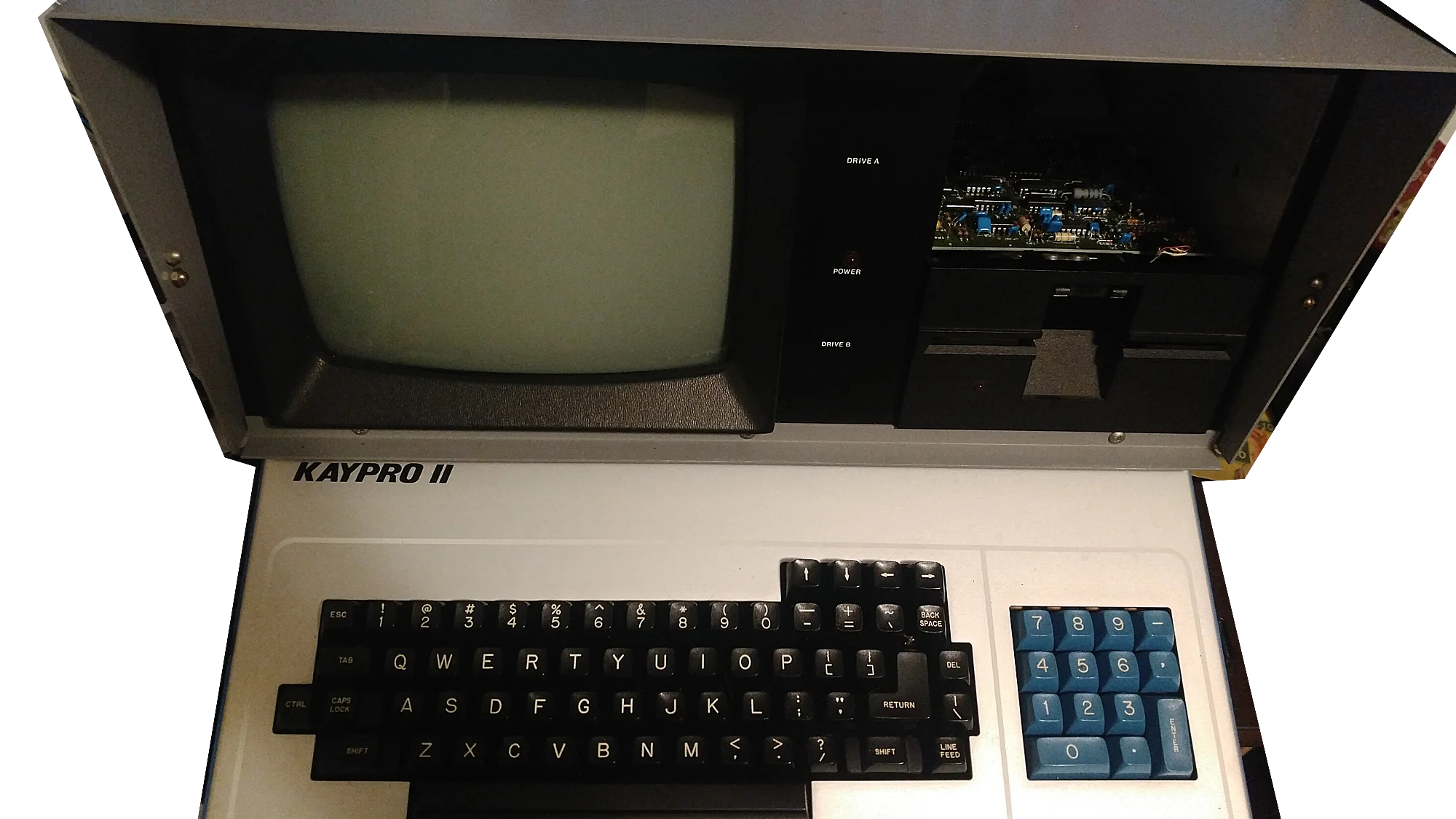
A few weeks ago, I stumbled upon an ad for a Kaypro II with dead floppy drives. For the cost of shipping, they were willing to give it away. As someone who loves luggables, I knew I had to have it. The Kaypro II has the following specs:
Z80 CPU @ 2.5MHz
64KB of RAM
2KB of ROM
Direct linear framebuffer access to VRAM
The seller was also nice enough to send a stack of 5.25" diskettes. I believe they have lost their magnetism, as (after fixing the Kaypro drives) the files on them were corrupted. So, I have to find another 5.25" drive that I can use to put images on the disks. In the meantime, why not hack the ROM?
Now, ROM hacking is new to me. I understand the concept, but do not have any of the required tools, such as an EEPROM reader. But I do have an Arduino, so I figured I could make it work. I started by digging up a schematic for the Kaypro II. Using this, I was able to derive the pinouts of the ROM chip. My understanding is that they follow a fairly standard layout, but I didn't want to risk that assumption on a nearly 40 year old part.

This is a picture of the ROM. When I first opened the Kaypro, there was nothing on the top of the IC. This is dangerous, as exposure to sunlight could wipe the chip! The first thing I did was put 2 layers of tape on to ensure it wouldn't be erased. The pinout is fairly simple, consisting of:
VCC and GND, used to supply power.
A set of address pins, used to tell it which byte you want to talk to. Since we have 2048 bytes, we need 11 address pins. 2^11 = 2048
A set of data pins, used to read to/write from the ROM. The system data bus is 8 bits wide, so there are 8 data pins.
A set of control pins, which handle everything else.
This ROM has 2 control pins we care about - OE and CE. OE, short for Output Enable, will tell the chip you want to read its internal memory. The other pin, Chip Enable, is used to enable/disable the chip. This is important when you have more than one component on the same bus - You need a way to differentiate them. Since we're only going to read the one ROM, we can pull this low(enabling the chip). Also, since we're only going to read, we can pull OE low as well.
So, the Arduino needs to output to the address bus, and read data off the data bus. I decided to wire pins 22 to 32 to the address bus, and pins 35 to 42 to the data bus. The pins on the ROM don't go in order like this, but it makes programming easier. And don't forget about the control pins! Remember, I tied them to GND.

This looks like a mess, but is as simple as I described above. It's just the sheer volume of wires that make it look complicated - promise! With that done, I was ready to start on the code.
I already knew what I wanted the code to do. It would write to the address bus, read from the data bus, send 1 byte over serial, increment the address bus, and repeat. This makes it easy to reconstruct an image from the ROM on the computer side. My final code looks like this:
  #define ROM_D0 35
  #define ROM_A0 22

  void setup()
  {
	  //data bus
	  for(int i = ROM_D0; i < ROM_D0 + 8; i++)
	  {
		  pinMode(i, INPUT);
	  }

	  //address bus
	  for(int i = ROM_A0; i < ROM_A0 + 11; i++)
	  {
		  pinMode(i, OUTPUT);
	  }

	  Serial.begin(57600);
  }

  void loop()
  {
	  char c;
	  for(int i = 0; i < 2048; i++)
	  {
		  //write to address bus
		  for(int a = ROM_A0; a < ROM_A0 + 11; a++)
		  {
			  digitalWrite(a, (i >> (a - ROM_A0)) & 1);
		  }
		  delay(10);
		  c = 0;
		  //read in the data bus
		  for(int d = ROM_D0; d < ROM_D0 + 8; d++)
		  {
			  c |= (digitalRead(d) == HIGH) << (d - ROM_D0);
		  }
		  Serial.print(c);
	  }

	  while(true) {}
  }
It's as simple as you'd imagine!
First, we set up the pins for what we need to do with them. We'll be reading from the data bus, so we set them as INPUT pins. We'll be writing to the address bus, so we set them as OUTPUT pins. It's important to get this right - Setting the data pins as OUTPUT, for instance, would cause the ROM chip and the Arduino to be pulling on the pins at the same time. If one pulled it high, and the other pulled it low, it could damage the chip, the Arduino, or both! We also initialize the serial port with a baud rate of 57600.
Next, we have the loop function, which is where the core of our code lives. A loop iterates our address counter. Each cycle, we use bitwise operators to turn the counter into a series of HIGHs and LOWs, which are placed on the address bus. A 10ms delay is placed so that the chip has time to update - I'm sure that it's significantly faster than this, but when you factor in the inductance of the rat's nest, I felt it was better to play it safe. Finally, we use bitwise operators to read the data bus into a char, which is sent over the serial port.
Amazingly, this worked! I went through the binary file it generated and could see text strings within it, such as "KAYPRO II" and "Please place your diskette into drive A". However, I was worried that my circuit may be unreliable, and I wanted to make sure it was good before I disassembled it. For this reason, I decided to download a Kaypro II ROM from the Internet, which was taken with an actual EPROM reader. Using a program called "z80-mon", I disassembled the machine code into Z80 assembler.
Here's a snippet of the code:
This is the code for enabling the floppy drive motors. I've added comments to explain how it works. Basically, it reads in from port 0x1C (The system port). It checks bit 6, which indicates the status of the floppy motor. The result is used to update the flag register. The next instruction, "RET Z", means "return from the function if the Zero flag is set", AKA if bit 6 is 0. If bit 6 is 1, the code continues. Next, bit 6 is set to 0, and then the resulting byte is written to the system port. Finally, the value 50 is put into register B, and the function at 0x425 is called. (It likely uses the value in B as an argument) There are over 1000 lines of Z80 assembler in total, so I'm not going to post it all here. It's in the git repo linked at the bottom!
My own Firmware
Doing some more disassembly, I found the code used to switch memory banks. I would need this to write to the screen, as the VRAM is located on bank separate from everything else. (Memory banking is used to increase the maximum amount of RAM that the CPU can access, by putting RAM into discrete "banks" which can be swapped in and out of the system busses.) I wrote a very basic program, which would copy a string off the ROM and into VRAM. Sounds simple, right? Unfortunately not. The VRAM is on bank 1, and the ROM is on bank 0. Because of this, I had to write some code to copy a string & executable binary into upper memory (which isn't affected by banking), and then jump to the newly-copied binary. This code would switch banks and copy the string from upper memory to the VRAM. And amazingly, it worked!
You can see there's lots of other garbage on the screen. This is because, when the computer turns on, the RAM isn't full of zeros. It randomly has zeros and ones scattered around - including in the VRAM. Since my program doesn't clear it, it shows up on the screen. In fact, even when booting on the stock firmware, there's a split second where the screen is full of random garbage characters just like with my program.
The last thing I want to do is read from the keyboard. Looking at the schematic, I found that it's connected through the serial chip. So, I added changes to my program so that it would wait for a byte to be available on channel B(the channel connected to the keyboard), and once it was, it would be read and copied onto the screen. Although simple in theory, I was unable to get it to function. I guess the serial port needs to be initialized in some way. I noticed that the firmware has some subroutines that write to port 12 as well as other undocumented ports. I have a feeling one of those will set up the serial devices - I guess I have to look over the schematic some more!
My debug process ended up looking like this:
Write the assembler code & assemble it into a flat binary file
(Optional) Run it in a simulator - it doesn't support the specific hardware connected to the Kaypro, so I was pretty limited here
Put an EEPROM chip in the breadboard programmer (Did I mention I had to write a new program for flashing the chip? Also, I was lucky enough to have a few spare 2K EEPROMs!)
Plug in the Arduino and flash the chip
Take the chip out of the breadboard and put it in the kaypro
Finally, boot the kaypro and see what happens!
As you can see, it's a very tedious process. I might design a proper PCB for the reader/programmer with a ZIF connector (if I go this route, I will probably make an adapter so I can stick a ZIF connector into the Kaypro's DIP socket). I'm still surprised it worked at all!